博文
[打听] 世界上第一只拍赫兹(PHz)光电晶体管 Petahertz phototransistor
||
[打听] 世界上第一只拍赫兹(PHz)光电晶体管 Petahertz phototransistor
一、石墨烯-硅-石墨烯晶体管
美国亚利桑那大学(University of Arizona)、加利福尼亚理工学院喷气推进实验室(Jet Propulsion Laboratory, California Institute of Technology)、德国 Ludwig-Maximilians-Universität München 人员合作研究,在 2025-05 公布了一种速度达 1.6 PHz(Petahertz phototransistor, 10^15)光电晶体管。
据报道,在石墨烯光电晶体管的两层石墨烯之间里加入一层特殊的硅层,实现了电子“隧穿”(电子几乎瞬间穿过石墨烯)。

图1 Fig. 1: Light-induced quantum current tunnelling in graphene phototransistor.
https://www.nature.com/articles/s41467-025-59675-5/figures/1
a The optical microscope (and zoom in) images of the graphene-silicon (Si)-graphene phototransistor and illustration of its band structure, the black dashed line presents the Fermi level. b The measured current-voltage (I–V) curve in case of laser ON (blue line) and laser OFF (red line). The inset shows the switching ON and OFF the photocurrent signal by the laser beam. c the tunnelling characteristics I–V curve for the Gr-Si-Gr transistor and the redline is an eye guide. The error bars present the calculated standard deviation error of three scans.
【机器翻译】 a 石墨烯-硅(Si)-石墨烯光电晶体管的光学显微镜(和放大)图像及其能带结构的图示,黑色虚线表示费米能级。b 激光器开启(蓝线)和激光器关闭(红线)时的测量电流-电压(I-V)曲线。插图显示了激光束对光电流信号的开启和关闭。c Gr-Si-Gr晶体管的隧穿特性I-V曲线和红线是一个视觉指南。误差条显示了三次扫描的计算标准偏差误差。
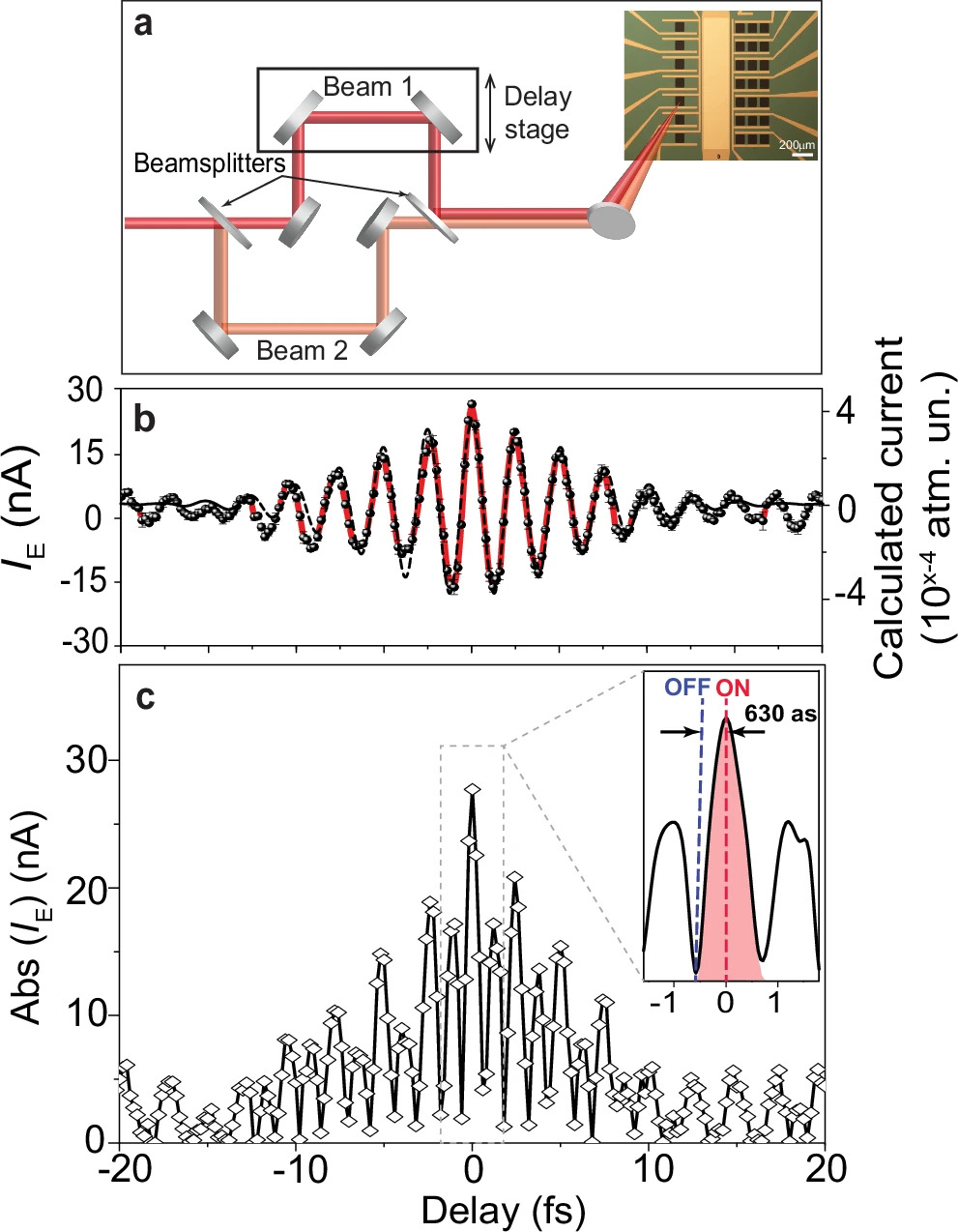
图2 Fig. 2: Attosecond current switching.
https://www.nature.com/articles/s41467-025-59675-5/figures/2
a Cross-correlation current measurement setup. The pump laser beam splits into two beams by beam splitter. The two beam are focused into the transistor and generate current signals. The delay between these two generated signals is controlled by a delay stage implemented in one of the beam paths. b Instantaneous field-induced current (IE) (average of three measurements), shown as black dots connected by red line. The error bars present the calculated standard deviation error of three scans. The calculated current is plotted in dashed black line. c Absolute IE measured signal modulation in time, obtained from (b), is plotted in diamond shape points connected with black line. The inset in (c) (a zoom in delay ranges from −1.5 to 1.5 fs) shows the switching of the current ON and OFF with a periodicity of 630 as.
【机器翻译】 a 互相关电流测量设置。泵浦激光束被分束器分成两束。两个光束聚焦到晶体管中并产生电流信号。这两个生成信号之间的延迟由在其中一个光束路径中实现的延迟级控制。b 瞬时场感应电流(IE)(三次测量的平均值),显示为用红线连接的黑点。误差条显示了三次扫描的计算标准偏差误差。计算出的电流以黑色虚线绘制。c 从(b)中获得的绝对IE测量信号随时间的调制,以与黑线连接的菱形点绘制。(c)中的插图(放大延迟范围为 -1.5 至 1.5 fs)示出了以630为周期的电流接通和关断的切换。
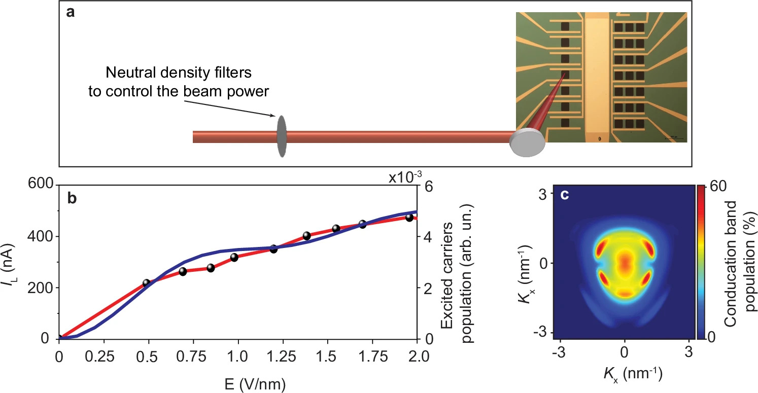
图3 Fig. 3: Controlling the light-induced current signal.
https://www.nature.com/articles/s41467-025-59675-5/figures/3
a Experimental setup illustration for controlling the light induced current in a graphene-silicon-graphene transistor. The laser beam of the pump pulse is focused by a parabolic mirror into a transistor channel. The power is controlled by a neutral density filter. b the measured light-induced current IL (black dots connect by red line) and the calculated excited carriers’ populations (blue line) as a function of the pump laser field intensity. c calculated carrier distribution in the reciprocal space (K) of graphene excited by 1.2 V/nm laser field.
【机器翻译】 a 用于控制石墨烯-硅-石墨烯晶体管中的光感应电流的实验设置图示。泵浦脉冲的激光束被抛物面镜聚焦到晶体管沟道中。功率由中性密度滤波器控制。b 作为泵浦激光场强度的函数的测量的光感应电流 IL (黑点由红线连接)和计算的激发载流子布居数(蓝线)。c 计算激发石墨烯倒数空间(K)中的载流子分布 1.2 V/nm激光场。
二、求:专业级科普
一时还没看明白是怎么回事。
请您给个“专业级”的科普。感谢!
参考资料:
[1] 新华网,2025-05-23 17:04:06,首个速度达拍赫兹光电晶体管问世
http://www.xinhuanet.com/liangzi/20250523/b217ba77de224fa48ace68ff7eb9289f/c.html
[2] Mohamed Sennary, Jalil Shah, Mingrui Yuan, Ahmed Mahjoub, Vladimir Pervak, Nikolay V. Golubev, Mohammed Th. Hassan. Light-induced quantum tunnelling current in graphene [J]. Nature Communications, 2025, 16(1): 4335
doi: 10.1038/s41467-025-59675-5
https://www.nature.com/articles/s41467-025-59675-5
[3] bilibili,2025-05-21 20:32:46,《今日科学》比现代电脑晶体管快100万倍的光电晶体管(常温常压光诱导的量
https://www.bilibili.com/video/BV1omJ6z3EXn/?vd_source=e95230c5ea5cb7f8d64c45d385caf46d
[4] 中国科学院,2025-05-22,首个速度达拍赫兹光电晶体管问世
https://www.cas.cn/kj/202505/t20250522_5069538.shtml
[5] 科普中国,2025-05-22,重新定义计算机处理能力极限首个速度达拍赫兹光电晶体管问世
https://www.kepuchina.cn/article/articleinfo?business_type=100&classify=0&ar_id=602719
[6] 2023-05-20,半导体光电子器件/semiconductor optoelectronic device/陈佳圭,中国大百科全书,第三版网络版[DB/OL]
https://www.zgbk.com/ecph/words?SiteID=1&ID=108818&Type=bkzyb&SubID=80676
以前的《科学网》相关博文链接:
[1] 2025-01-28 02:23,[小资料,科普,要点] “电子瓶颈”、“集成光路的瓶颈(集成光路瓶颈)”
https://blog.sciencenet.cn/blog-107667-1470711.html
[2] 2025-04-30 23:46,[打听,资料] 集成光学芯片商业化:集成光路瓶颈克服了吗?(关联:integrated large-scale photonic)
https://blog.sciencenet.cn/blog-107667-1484117.html
[3] 2025-09-05 20:39,[新闻,资料,科普] Nature 2025:模拟光学计算机及其应用
https://blog.sciencenet.cn/blog-107667-1500656.html
[4] 2025-01-03 22:52,[打听,讨论] 谁是未来的主要计算机:超导、纳米(纳米管技术)、光学(光子)、DNA(生物)、量子计算机等
https://blog.sciencenet.cn/blog-107667-1467265.html
[5] 2025-01-27 22:27,[打听,资料] 2nm节点光刻J,还使用“浸入式光刻技术 immersion lithography technology”吗?
https://blog.sciencenet.cn/blog-107667-1470704.html
[6] 2025-06-18 22:20,[打听,笔记,优先权] “光点击化学 photoclick chemistry”是一种“可编程”的计算(信息处理)? (关联:“自然运算”)
https://blog.sciencenet.cn/blog-107667-1490360.html
[7] 2024-07-18 22:50,[请教] 《物理学》里光子(光量子)能量 E=hν 精确成立的条件是什么?
https://blog.sciencenet.cn/blog-107667-1442847.html
感谢您的指教!
感谢您指正以上任何错误!
感谢您提供更多的相关资料!
https://blog.sciencenet.cn/blog-107667-1521868.html
上一篇:[从前(12),创新,原创] 半发面的芝麻烧饼
下一篇:[老家,饮食,文化] 河北省灵寿县的缸炉烧饼
