博文
[小资料] 1949年肖克莱(William Bradford Shockley)的结型晶体管论文的引言(图片)和图片页
||
[小资料] 1949年肖克莱(William Bradford Shockley)的结型晶体管论文的引言(图片)和图片页
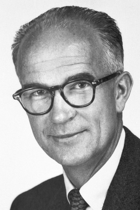
肖克莱 William Bradford Shockley, 1910-02-13 ~ 1989-08-12
The Nobel Prize in Physics 1956
https://www.nobelprize.org/prizes/physics/1956/shockley/facts/
https://www.nobelprize.org/prizes/physics/1956/summary/
一、肖克莱:从“场效应管”到“结型晶体管”
1945年开始,肖克莱和布拉坦(Walter Houser Brattain)开始研制“绝缘栅场效应管”,可惜没有成功。半导体场效应管的专利,1926-10-08 由利林菲尔德(Julius Edgar Lilienfeld)申请,1930-01-28 授权。
1947-12-15 巴丁(John Bardeen)、布拉坦(Walter Houser Brattain)制作出第一只“点接触晶体管 pointcontact transistor”。
1948-01-23 肖克莱提出了采用 Russell Ohl 发明的PN结来制作晶体管的设想。“PN结晶体管”比“点接触晶体管”晚了一个多月。
1951-04 贝尔实验室的 Gordon Teal 、Morgan Sparks 制作出第一只结型晶体管。
1951-07-04 贝尔实验室公布了结型晶体管发明。
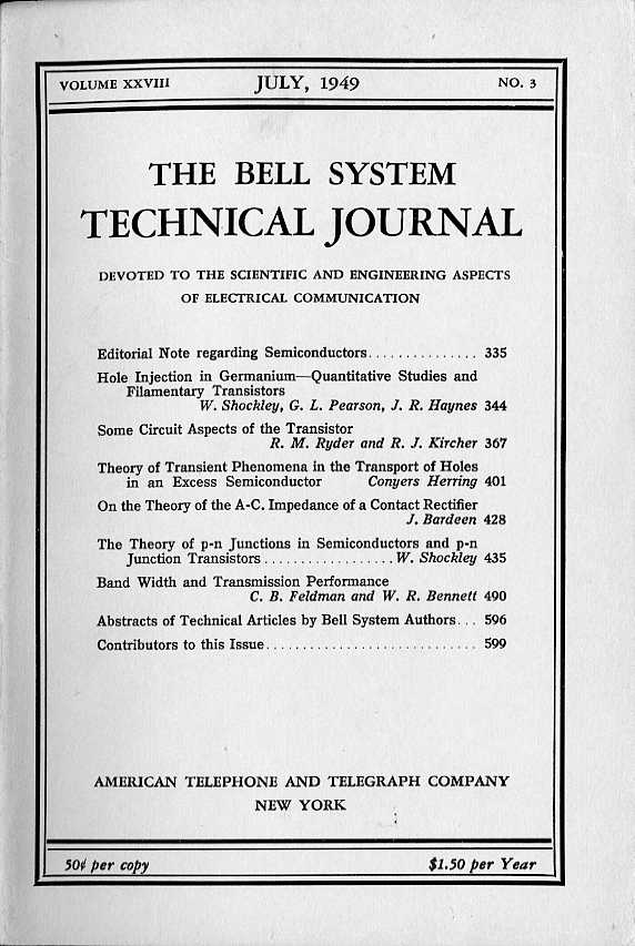
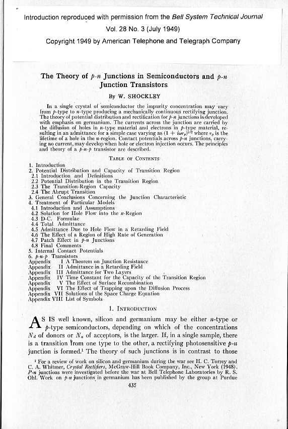
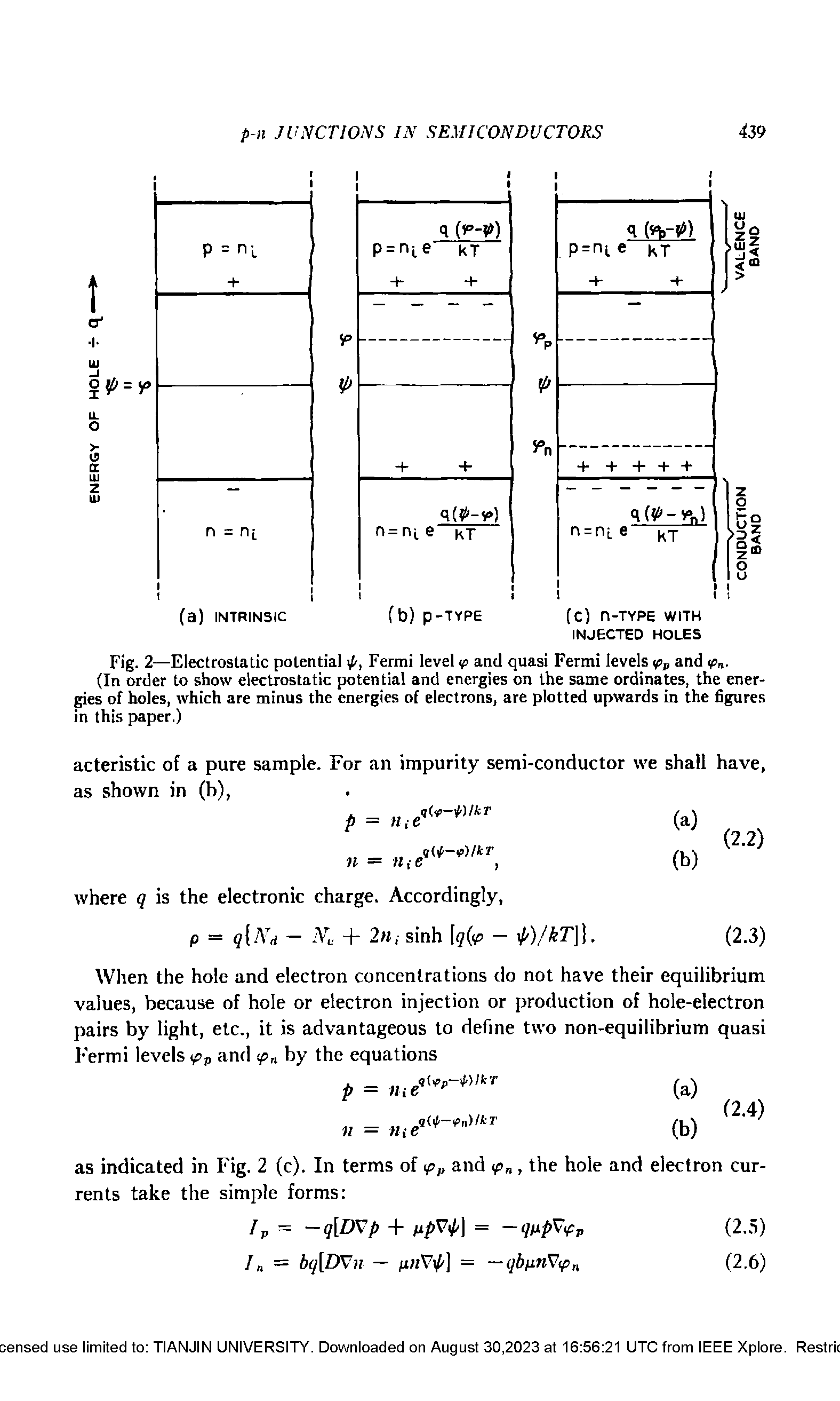
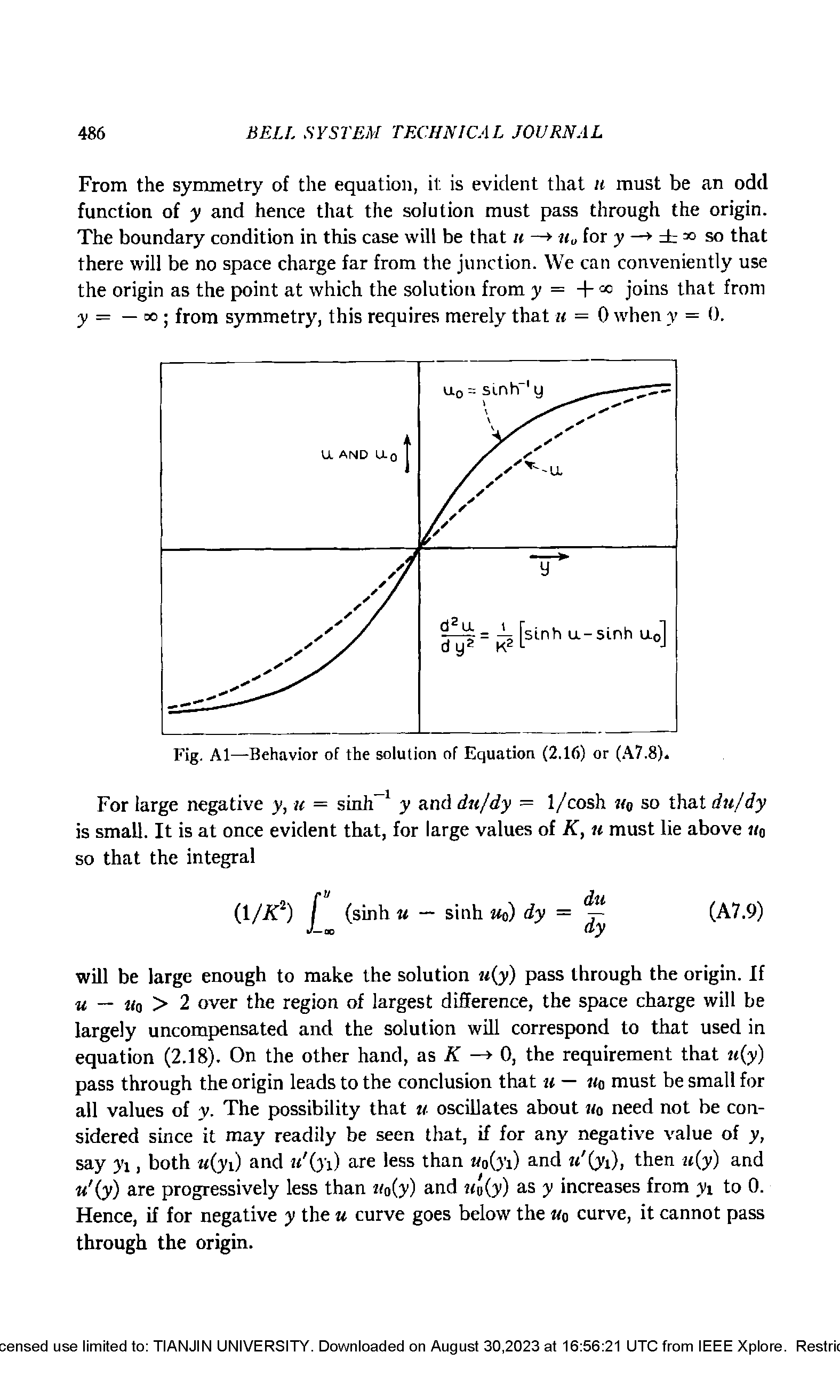
二、1949年肖克莱的论文《The Theory of P-N Junctions in Semiconductors and P-N Junction Transistors 半导体中的P-N结理论和P-N结晶体管》引言部分和有图片的页
1949-07 肖克莱在《The Bell System Technical Journal》发表论文“The Theory of P-N Junctions in Semiconductors and P-N Junction Transistors 半导体中的P-N结理论和P-N结晶体管”,提出了“结型晶体管”。
肖克莱该文的全文 55 页。下面只贴出引言和有图片的页。
CHM, Computer History Museum
的
RESOURCES
CLASSIC SEMICONDUCTOR PAPERS AND PATENTS
里,有肖克莱 1949-07 论文《The Theory of P-N Junctions in Semiconductors and P-N Junction Transistors 半导体中的P-N结理论和P-N结晶体管》引言部分。
1949 - Shockley's seminal paper on P-N junction devices
Shockley, William. "The Theory of P-N Junctions in Semiconductors and P-N Junction Transistors" Bell System Technical Journal Vol. 28 No. 3 (July 1949) (Introduction only)
http://s3.computerhistory.org/siliconengine/shockley-pn-junction.pdf
https://www.computerhistory.org/siliconengine/resources/
其余图片页来自 IEEE。
图片形式如下:
(1)
(2)

(3)

(4)

(5)
(6)

(7)
(8)
(9)
(10)
(11)
(12)
(13)
(14)
(15)
(16)
三、肖克莱、诺伊斯
肖克莱提出的结型晶体管、场效应管,是后来工业化生产采用的晶体管。
但巴丁、布拉坦的“点接触晶体管”,是方向性的大发现。
在后来的集成电路里又有类似的现象:
基尔比的集成电路。连线是露在外面的。不利于工业生产。
稍微晚点的诺伊斯的集成电路,采用了平面工艺,导线采用“蒸发淀积金属”直接制作成内部连线。这是后来工业生产里集成电路的主流。
在目前“半电路、半电磁场”研制中,美国学者的“串音”,相当于“点接触晶体管”、基尔比的集成电路。主要是证明“此路可通”。看上去不是真正工业化设计、生产的好方法。
“半电路、半电磁场”电路,下一步的突破在哪里?真正适合工业化设计、生产,还是需要什么?
参考资料:
[1] 宋德生. 信息革命的技术源流[M]. 成都: 四川人民出版社, 1986-04.
[2] 童诗白. 世纪回眸:纪念晶体管的发明和由此引出的启发[J]. 电气电子教学学报, 2001, 23(3): 3-6. 2001年6月
http://www.cqvip.com/QK/98031A/200103/5280096.html
俗语说:“人过三十五,难有大建树”。但是,晶体管发明时,巴、布、肖三人分别是39岁、45岁、37岁,都已超龄,而巴第二次获诺贝尔物理学奖所做的超导研究是在他48岁时。因此,年龄不是主要的障碍,只要我们思路正确,刻苦钻研,败而不馁,锲而不舍,善于抓住机遇,就一定会有所成就。
[3] Electronics Timeline, 20th century's greatest engineering achievements
http://www.greatachievements.org/?id=3956
[4] Greatest Engineering Achievements of the 20th Century
http://www.greatachievements.org/
[5] 1948: CONCEPTION OF THE JUNCTION TRANSISTOR
WILLIAM SHOCKLEY CONCEIVES AN IMPROVED TRANSISTOR STRUCTURE BASED ON A THEORETICAL UNDERSTANDING OF THE P-N JUNCTION EFFECT.
https://www.computerhistory.org/siliconengine/conception-of-the-junction-transistor/
[6] 1951: FIRST GROWN-JUNCTION TRANSISTORS FABRICATED
GORDON TEAL GROWS LARGE SINGLE CRYSTALS OF GERMANIUM AND WORKS WITH MORGAN SPARKS TO FABRICATE AN N-P-N JUNCTION TRANSISTOR.
https://www.computerhistory.org/siliconengine/first-grown-junction-transistors-fabricated/
[7] 1949 - Shockley's seminal paper on P-N junction devices
Shockley, William. "The Theory of P-N Junctions in Semiconductors and P-N Junction Transistors" Bell System Technical Journal Vol. 28 No. 3 (July 1949) (Introduction only)
http://s3.computerhistory.org/siliconengine/shockley-pn-junction.pdf
[8] The Nobel Prize in Physics 1956, The Nobel Foundation
https://www.nobelprize.org/prizes/physics/1956/summary/
[9] 1926: FIELD EFFECT SEMICONDUCTOR DEVICE CONCEPTS PATENTED
JULIUS LILIENFELD FILES A PATENT DESCRIBING A THREE-ELECTRODE AMPLIFYING DEVICE BASED ON THE SEMICONDUCTING PROPERTIES OF COPPER SULFIDE. ATTEMPTS TO BUILD SUCH A DEVICE CONTINUE THROUGH THE 1930S.
https://www.computerhistory.org/siliconengine/field-effect-semiconductor-device-concepts-patented/
[9] EDN, 2019-10-08, Lilienfeld patents field effect transistor, October 8, 1926
https://www.edn.com/lilienfeld-patents-field-effect-transistor-october-8-1926/
Lilienfeld’s patent for a “method and apparatus for controlling electric currents” was granted on January 28, 1930.
[10] TIMELINE, Computer History Museum
https://www.computerhistory.org/siliconengine/timeline/
[11] W. Shockley. The theory of p-n junctions in semiconductors and p-n junction transistors [J]. The Bell System Technical Journal ( Volume: 28, Issue: 3, July 1949), 1949, 28(3): 435-489.
doi: 10.1002/j.1538-7305.1949.tb03645.x
https://ieeexplore.ieee.org/document/6773080/citations#citations
https://onlinelibrary.wiley.com/doi/10.1002/j.1538-7305.1949.tb03645.x
[12] RESOURCES, Computer History Museum
https://www.computerhistory.org/siliconengine/resources/
[13] Wei Cao, Huiming Bu, Maud Vinet, Min Cao, Shinichi Takagi, Sungwoo Hwang, Tahir Ghani, Kaustav Banerjee. The future transistors [J]. Nature, 2023, 620(7974): 501–515. 16 August 2023
doi: 10.1038/s41586-023-06145-x
https://www.nature.com/articles/s41586-023-06145-x
[14] Sah Chih-Tang (萨支唐). Evolution of the MOS transistor-from conception to VLSI [J]. Proceedings of the IEEE, 1988, 76(10): 1280 - 1326. October 1988
doi: 10.1109/5.16328
https://ieeexplore.ieee.org/document/16328
[15] Who Invented the Transistor? Computer History Museum, 2013-12-04, David Laws
https://computerhistory.org/blog/who-invented-the-transistor/
相关链接:
[1] 2023-08-30,[小资料] 1948年巴丁、布拉坦(Bardeen, Brattain)的点接触晶体管专利(图片)
https://blog.sciencenet.cn/blog-107667-1400907.html
[2] 2023-08-29,[小资料] 1959年霍尔尼(Jean Amedee Hoerni)的平面工艺专利(图片)
https://blog.sciencenet.cn/blog-107667-1400737.html
[3] 2023-08-28,[小资料] 1959年诺伊斯(Robert Norton Noyce)的集成电路专利(图片)
https://blog.sciencenet.cn/blog-107667-1400618.html
[4] 2023-08-27,[小资料] 1959年基尔比(Jack St. Clair Kilby)的集成电路专利(图片)
https://blog.sciencenet.cn/blog-107667-1400524.html
[5] 2022-09-19,[???] 热血沸腾之后,更是“耗尽/耗干”后的无奈(关联资料“集成电路”,诺伊斯 Robert Noyce)
https://blog.sciencenet.cn/blog-107667-1356020.html
[6] 2023-08-02,[小资料] 1952年杜默(G. W. A. Dummer)提出“集成电路概念 Integrated Circuit Concept”
https://blog.sciencenet.cn/blog-107667-1397631.html
[7] 2023-05-01,“五一”国际劳动节:真空管 → 晶体管、集成电路 → “半电路、半电磁场”电路 → ……
https://blog.sciencenet.cn/blog-107667-1386442.html
[8] 2019-07-17,[求助] 集成电路 Integrated Circuit 当前最新技术资料?
https://blog.sciencenet.cn/blog-107667-1189948.html
[9] 2019-07-14,有关集成电路 Integrated Circuit 的网页
https://blog.sciencenet.cn/blog-107667-1189467.html
[10] 2019-03-17,[建议] 关于集成电路中研制可变电阻的建议
https://blog.sciencenet.cn/blog-107667-1168144.html
[11] 2019-07-07,有关 Geoffrey W. A. Dummer 先生的网页
https://blog.sciencenet.cn/blog-107667-1188470.html
[12] 2019-07-13,有关 Mervin Joe Kelly 先生的网页
https://blog.sciencenet.cn/blog-107667-1189385.html
[13] 2019-07-01,[请教] 量子集成电路、量子芯片 Quantum Chip 今后30年内的实用前景?
https://blog.sciencenet.cn/blog-107667-1187623.html
[14] 2021-08-10,[求证] ASML 腾飞的技术原因是什么?【immersion system】
https://blog.sciencenet.cn/blog-107667-1299147.html
[15] 2022-09-24, 《信息革命的技术源流》第三轮阅读:创新真难!
https://blog.sciencenet.cn/blog-107667-1356669.html
[16] 2023-08-21,[征求意见稿] “半电路、半电磁场”电路:目标和现状
https://blog.sciencenet.cn/blog-107667-1399839.html
感谢您的指教!
感谢您指正以上任何错误!
感谢您提供更多的相关资料!
![(热门)[小资料] 1949年肖克莱(William Bradford +1.jpg](http://image.sciencenet.cn/home/202309/02/010605d608mh16epez5yc9.jpg)
https://blog.sciencenet.cn/blog-107667-1401002.html
上一篇:[小资料] 1948年巴丁、布拉坦(Bardeen, Brattain)的点接触晶体管专利(图片)
下一篇:[小资料] 1926年利林费尔德(Julius Edgar Lilienfeld)的场效应半导体专利(图片)