博文
刊·见 | International Journal of Optomechatronics引领智能光学与精密机械交叉  精选
精选
||
在科技融合创新的时代浪潮中,光机电一体化技术正成为推动多领域突破的核心动力。光学元件的精密控制、机械系统的微型化集成、流体力学与电子技术的交叉应用,已深度渗透至天文观测、生物医学成像、先进制造等战略领域。
本期【刊•见】为诸位介绍聚焦光机电一体化技术领域的国际期刊International Journal of Optomechatronics。除了对关键指标进行详尽解读外,还将向您介绍刊内近三年高被引文章,以及近一年高阅读量文章:
 Online ISSN: 1559-9620 Print ISSN: 1559-9612
International Journal of Optomechatronics 期刊发表涵盖光学、力学、流体学和电子学等多学科的研究成果。重点研究领域包括但不限于:自适应光学;光力学;机器视觉、跟踪与控制;基于图像的微/纳米操纵;光机电一体化控制工程;光学计量学;基于光学与视觉的制造、工艺、监测及控制等。
该期刊已被SCIE、Scopus和CSA Technology Research Database 等核心数据库收录。
根据JCR显示,International Journal of Optomechatronics
在工程学、电气与电子学领域排名 198/368
在工程学、机械工程领域排名 81/182
在光学领域排名 67/125
根据Scopus显示,International Journal of Optomechatronics
2024年CiteScore为 7.2
在物理与天文学:仪器仪表学领域排名 25/174
在工程学:机械工程领域排名 121/720
在工程学:电气与电子工程领域排名 175/970
根据2025年3月20日发布的中国科学院文献情报中心期刊分区表显示,International Journal of Optomechatronics
大类及分区:工程技术2区
小类及分区:
工程:机械2区
工程:电子与电气3区
光学3区
作者须知接收文章类型
International Journal of Optomechatronics 期刊接受原创研究论文和技术报告,编辑及编委会会定期征集综述文章和特邀稿件。
审稿周期
从提交稿件到获取初审意见,平均需要19天
稿件接受率:17%
文章出版费(APC)
请访问期刊主页或Taylor & Francis Open Access APC Cost Finder查找适用于作者所在国家及不同文章类型的费用情况。若您所在的机构或相关资助者与我们签有开放获取出版协议,您可能有资格获得APC支持,请访问我们的作者服务网站以了解更多!
Taylor & Francis现在开通APC便捷支付功能,可以一键通过微信、支付宝和银联使用人民币便捷付款。
编辑团队International Journal of Optomechatronics 期刊主编由来自意大利梅西纳大学的Giovanni Crupi教授担任,副主编汇聚来自英国、美国、德国、新加坡等地的领域专家,编委团队由德国、中国、加拿大等多地的行业翘楚组成。
期刊主编
Giovanni Crupi
Giovanni Crupi,意大利梅西纳大学(University of Messina)教授,主要研究领域包括用于无线通信应用的先进电子器件的微波特性表征与建模,以及用于生物工程应用的传感器的微波特性表征与建模。
作者分布根据JCR显示,近三年在International Journal of Optomechatronics 发文的国家/地区中,发文比较活跃的是:
中国
韩国
新加坡
近三年,在International Journal of Optomechatronics 发文的全球高校和科研机构中,发文比较活跃的是:
韩国大邱庆北科学技术院
新加坡国立大学
马来西亚国立大学
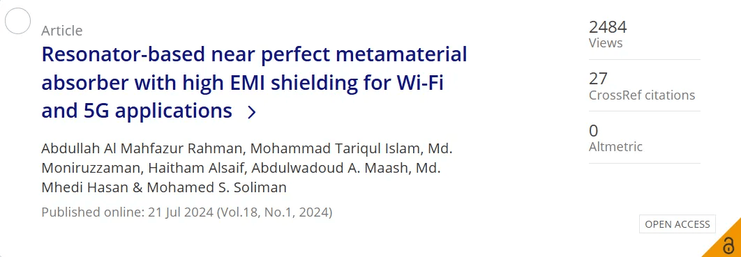
基于共振器的近乎完美的超材料吸收体,具有高电磁干扰屏蔽性能,适用于Wi-Fi和5G应用
通讯作者:Abdullah Al Mahfazur Rahman et al.
文章摘要:
This paper introduces a perfect metamaterial absorber (MMA) achieving exceptional electromagnetic signal absorption at application-oriented frequencies of 2.40 and 3.50 GHz in addition to 6.09 GHz. The MMA exhibits absorption rates of 99.85, 98.6, and 96.7%, with high shielding effectiveness (SE) of 36.44, 32.58, and 31.13 dB against electromagnetic interference (EMI) at those frequencies. The structure of the copper resonator on the FR4 substrate allows the on-design frequency switching from 3.43 to 3.70 and 5.65 to 6.55 GHz, respectively. The structural symmetry enables polarization and incidence angle independence up to 60° for both transverse electric and magnetic modes. The perfect absorption of the MMA is shown by the near-zero polarization conversion ratio. There is an adjacent correlation between the measurement and simulation results. The proposed MMA emerges as an efficient EMI shield for Wi-Fi and 5G signals, offering perfect absorption and extensive polarization characteristics.
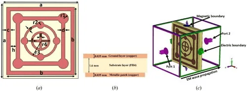
Figure 1. (a) Different dimensions of the resonator, (b) three layers of the MMA, and (c) simulation boundaries with wave source.
基于Ni-PI-Ni的纳米构筑体近乎完美的超材料吸收器,具有入射角稳定性,适用于可见光和近红外应用
作者:Abu Hanif et al.
文章摘要:
This article presents a wideband metamaterial absorber (WMMA) for the visible and near-infrared (NIR) region application. The proposed metamaterial absorber comprises three layers of sandwiched (metal-dielectric-metal) model based on Nickel-Polyamide-Nickel. The multiple resonators on top layers achieve an average absorption of 98.16% over a range from 380 to 2300 nm with a compact unit cell size of 100 × 100 × 42 nm3. The designed WMMA shows 99% perfect absorption for a large bandwidth of 685 nm. Considering its wideband absorption, the physical absorption phenomenon was also explained in terms of the proposed WMMA's surface electric field, magnetic field, and current distribution. Also, the effects of materials and structural parameters on absorption performance with a FOM have been studied. The absorption performance is analysed with various polarization angles to demonstrate polarization insensitivity. The designed WMMA shows the absorption of >70% at large incident angles of 70°. The perceptible contribution of this WMMA is large unity absorption bandwidth at visible to NIR region with high incident angle stability, polarisation insensitivity, thermal robustness of the constituting metal and simple nanostructure geometry. Therefore, the proposed WMMA has good potential in sensors, thermal emitters, photodetectors, and absorber applications.

Figure 1. (a) The schematic of the proposed WMMA, (b) simulated absorption, reflection, and transmission of the proposed WMMA.
近一年内高阅读量文章
作者:Ching Lin Li et al.
文章摘要:
The demand for high-power, high-density VCSEL light sources in applications such as space, artificial intelligence, silicon photonics, and autonomous vehicles is steadily increasing. VCSEL chips are epitaxially grown on GaAs substrates and then packaged by attaching them to a mounting bracket using high-temperature-resistant adhesives. This issue limits the VCSEL’s output power, and restricts its application range. We propose first removing the VCSEL epitaxial layer from the GaAs substrate and transferring it to a CuW substrate. The VCSEL chip is then mounted on an AlN substrate using a metal eutectic bonding technique. The results indicate that bonding 36 VCSELs with a wavelength of 840 nm to CuW chips and mounting them onto an AlN substrate to form an array achieved voltage of 8.59 V and a driving current of 18 A. The output optical power reached 57.68 W, with a reduced packaging thermal resistance of 0.232 K/W.
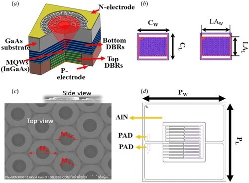
Figure 1. VCSEL chip, (a) Schematic of the epitaxial structure of the VCSEL chip, (b) 2D schematic of the VCSEL chip dimensions, (c) SEM image of the VCSEL chip, and (d) 2D schematic of the VCSEL array light board.
https://blog.sciencenet.cn/blog-3574014-1531127.html
上一篇:从被拒稿到录用:写英语Literature Review的“避坑+加分”指南
下一篇:论文Accepted指南:论文Result部分这样写,才是写到审稿人心坎里
