博文
[转载]CPB封面文章和亮点文章 | 2025年第9期
||

Acoustic detection of high-resistance states in gated bilayer graphene devices
Guo-Quan Qin(秦国铨), Yi-Bo Wang(王奕博), Guo-Sheng Lei(雷国盛), Zhuo-Zhi Zhang(张拙之), Xiang-Xiang Song(宋骧骧), and Guo-Ping Guo(郭国平)
Chin. Phys. B, 2025, 34 (9): 097201

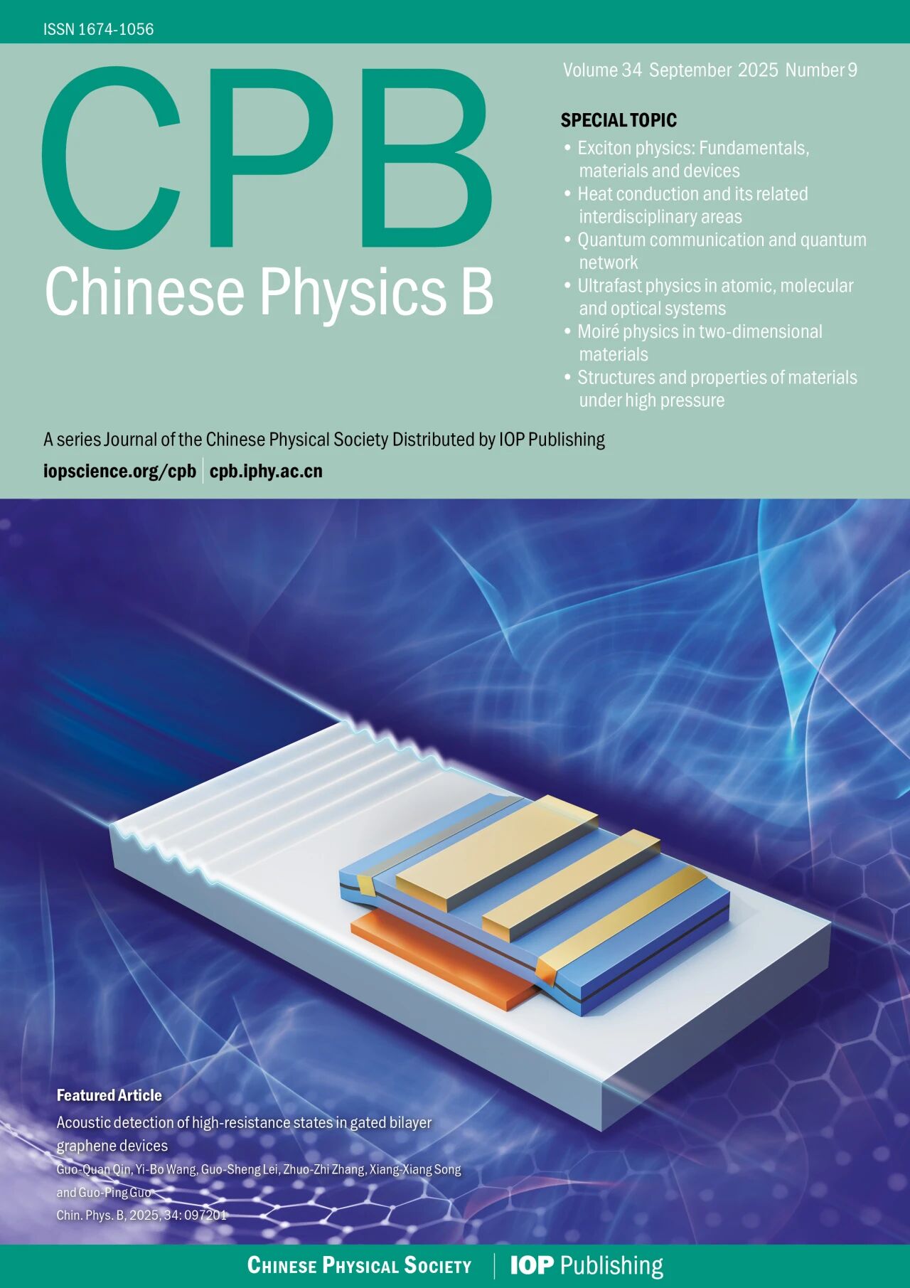
在双层石墨烯中施加垂直电场,可以打开一个电学可调的带隙,并诱导出高阻态。该高阻态能彻底夹断导电沟道,对于制备高性能栅控器件至关重要。然而,正是由于其极高的电阻,特别是当器件中不同区域处于不同的高阻态时,传统的电学测量方法难以对这些高阻态进行精确表征和有效分辨。
为解决这一挑战,本研究利用声表面波与石墨烯中载流子之间的强声电效应,实现了对多栅极双层石墨烯器件中高阻态的声学探测。实验表明,在不同栅压配置下产生的电阻相近(均约10^8 Ω)的高阻态,其声电响应却展现出迥异的特征,可用于甄别不同高阻态。尤为重要的是,本研究展示了一项电学测量难以实现的功能:当器件的导电沟道被一个顶栅彻底夹断后,另一个顶栅的调控作用仍然可以被声表面波探测到。这一结果充分展示了利用声表面波探测高阻态的独特能力与广阔前景。
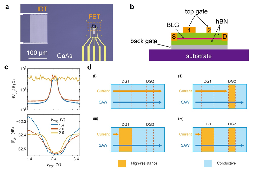
Fig. 1. (a) Optical microscope image of the device. The interdigital transducers (IDTs) are used for actuating surface acoustic waves (SAWs) on the piezoelectric substrate of GaAs. The cross-sectional schematics of the multi-gated field-effect transistor (FET) based on bilayer graphene (BLG) is illustrated in (b). (c) Electrically (upper panel) and acoustically (lower panel) measured results. When the conducting channel is pinched off by one top gate TG2 (the yellow curve), the gating effect of another top gate TG1 can be acoustically, but not electrically, detected. (d) Since high-resistance states can be achieved in both dual-gated regions DG1 and DG2, and are connected in series, traditional electrical measurements only detect whether the conducting channel is pinched off, thus failing to distinguish cases (ii), (iii), and (iv). However, the acoustic detection not only enables identification of high-resistance states underneath different top gates with different widths (between cases (ii) and (iii)), but also responds differently upon gating even when the conducting channel is already pinched off by another top gate (between cases (ii) and (iv)).

Optically-excited acoustic waves in Si nanowires probed by time-resolved HOLZ lines
He Wang(王贺), Shuaishuai Sun(孙帅帅), Yizhe Wang(王怡哲), Qianming An(安乾明), Xianhui Ye(叶显珲), Jun Li(李俊), Huanfang Tian(田焕芳), Huaixin Yang(杨槐馨), Jianqi Li(李建奇), and Zian Li(李子安)
Chin. Phys. B, 2025, 34 (9): 098701

近年来,超快电子显微镜(UTEM)技术为材料结构与电子动力学研究提供了重要手段。随着微型声学器件的快速发展,纳米尺度声波传播行为的精确探测需求日益迫切。本研究围绕纳米结构中声波探测的技术难点,利用UTEM在单根硅纳米线中光学激发声波,采集会聚束电子衍射(CBED)条件下高阶劳厄线(HOLZ)的响应信号,并构建几何模型,重点考察了基于HOLZ数据完整重构形变梯度张量的可行性。
研究发现,单个晶带轴CBED实验在反演形变梯度张量时存在本征模糊性,不同张量可能导致高度相似的衍射图案。通过实验与模拟结果的比对,验证了所建几何模型的可靠性。通过引入离轴CBED图像采集方式,HOLZ线可见度得到显著提升,为纳米结构中声波传播的空间分辨分析提供了可靠方法。本工作所发展的方法实现了纳米尺度应变波传播的高时空分辨率测量,为先进材料的微观表征提供了时间分辨的新方案。
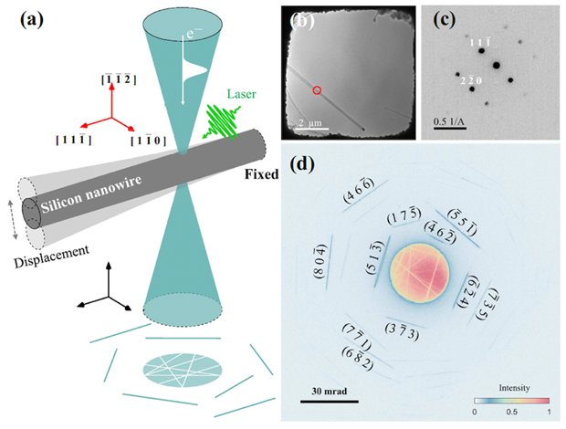
Fig. 1. An optically excited Si NW probed by time-resolved (tr-) HOLZ lines under CBED conditions. (a) Schematic representation of the experimental setup with the microscope XYZ coordinate system and the Miller indices lattice coordinate system. (b) Bright-field TEM image of the Si NW with one end fixed on the Cu grid. The red circle denotes the area for
HOLZ line recording. (c) Selected area electron diffraction pattern taken along the [112] zone-axis. (d) Off-zone-axis CBED pattern taken along a direction deviating from the exact [112] zone-axis, for better visibility of the HOLZ lines.

Superconductivity and band topology of double-layer honeycomb structure M2N2 (M=Nb, Ta)
Jin-Han Tan(谭锦函), Na Jiao(焦娜), Meng-Meng Zheng(郑萌萌), Ping Zhang(张平), and Hong-Yan Lu(路洪艳)
Chin. Phys. B, 2025, 34 (9): 097402

在凝聚态物理领域,二维双层蜂窝 (DLHC) 结构材料因其独特的物理性质而备受关注,但超导性在这类结构中尚未被发现。本文聚焦于具有双层蜂窝结构的M2N2(M = Nb, Ta)材料,采用第一性原理计算方法,系统研究其超导特性与能带拓扑性质。研究发现,Nb2N2和Ta2N2展现出优异的动力学和热力学稳定性,均为金属性材料且具有超导性,其超导转变温度(Tc)分别为6.37 K和8.80 K。超导源于过渡金属d轨道电子与低频过渡金属主导的声子模式之间的电声耦合。此外,这两种材料均具有非平庸的能带拓扑特性,其拓扑Z2指数为1,并存在受拓扑保护的边缘态。
本研究首次在双层蜂窝结构中揭示了由电声耦合诱导的超导现象,填补了该体系在超导研究领域的空白。同时,这项工作为探索超导与拓扑之间的相互作用提供了理想平台,并为设计兼具超导和拓扑特性的新型二维材料提供了重要的理论指导和实验参考,具有重要的科学意义和应用前景。
Fig. 5. Phonon dispersion of (a) Nb2N2 and (e) Ta2N2 weighted by the vibration modes of M and N atoms, respectively. (b), (f) Phonon dispersion weighted by the magnitude of EPC λqν. The insets show the vibration modes for the prominent λqν I for Ta2N2. The brown and gray spheres represent Ta and N atoms, respectively. (c), (g) Total and atom-projected phonon DOS for Nb2N2 and Ta2N2. (d), (h) Eliashberg spectral function α2F(ω) and cumulative frequency dependence EPC function λ(ω) for Nb2N2 and Ta2N2.

Strain tuning of the transport gap and magnetic order in Dirac fermion systems
Jingyao Meng(孟敬尧), Zenghui Fan(范增辉), Miao Ye(叶苗), and Tianxing Ma(马天星)
Chin. Phys. B, 2025, Vol. 34(9): 098101

石墨烯作为典型的Dirac费米子体系,其本征零带隙特性严重限制了其在电子与光电器件中的应用。如何有效打开并调控其能隙,是当前二维材料研究中的关键挑战。本文通过行列式量子蒙特卡洛模拟,系统研究了在非均匀应变作用下石墨烯的电子输运与磁序演变,揭示了该应变在调控其电子态与磁性方面的双重作用。
研究发现,沿zigzag方向施加非均匀应变,可在弱关联区域诱导金属-绝缘体转变,打开输运能隙;而在强关联区域,应变则可破坏反铁磁序,实现从Mott绝缘体到非磁性绝缘体的转变。尤为重要的是,电子关联作用显著降低了打开能隙所需的临界应变,而增强相互作用则提升了破坏磁序的应变阈值。此外,研究还发现掺杂会抑制能隙的打开,为多物理场调控提供了新思路。
该工作不仅揭示了一种非均匀应变在二维Dirac材料中的相图调控机制,也为应变工程在石墨烯基晶体管、传感器和自旋电子器件中的应用提供了理论依据与设计指导。
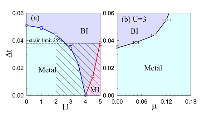
Fig. 1. Phase diagram of the strained honeycomb superlattice: (a) the competitive phases among metal, band insulator (BI) and Mott insulator (MI) at half-filling under the interplay of on-site interaction U and strain parameter Δt, which contains a graphene-supported area (slash area) under strain limit 25%; and (b) the doping effect with Δt at U=3. The critical points are derived from the data of conductivity and AFM spin structure factor at (a), while of DOS with varying chemical potential at (b).

Instrumentation and Measurement
Computational Programs for Physics

Celebrating 30 Years of Chinese Physics B
Stephen J. Pennycook: A research life in atomic-resolution STEM and EELS
Recent progress on kagome metals and superconductors
Moiré physics in two-dimensional materials
Computational programs in complex systems
Quantum computing and quantum sensing
Structures and properties of materials under high pressure
Post-Moore era: Materials and device physics
States and new effects in nonequilibrium
Smart design of materials and design of smart materials
Superconductivity in vanadium-based kagome materials

长按二维码,关注我们
https://iopscience.iop.org/journal/1674-1056
https://blog.sciencenet.cn/blog-3377544-1509334.html
上一篇:[转载]CPB2025年第9期文章目录(五)
下一篇:[转载]数据论文〡高通量筛选的Kagome超导体数据集
