博文
[转载]CPB亮点文章 | 2025年第7期
||

亮点文章
Hao Chen(陈浩), Jumin Shi(史聚民), Xiangyu Luo(罗翔宇), Yinghao Li(李颖昊), Yiwen Chen(陈逸雯), Chaohui Yin(殷超辉), Yingjie Shu(束英杰), Jiuxiang Zhang(张九相), Taimin Miao(苗泰民), Bo Liang(梁波), Wenpei Zhu(朱文培), Neng Cai(蔡能), Xiaolin Ren(任晓琳), Chengtian Lin(林成天), Shenjin Zhang(张申金), Zhimin Wang(王志敏), Fengfeng Zhang(张丰丰), Feng Yang(杨峰), Qinjun Peng(彭钦军), Zuyan Xu(许祖彦), Guodong Liu(刘国东), Hanqing Mao(毛寒青), Xintong Li(李昕彤), Lin Zhao(赵林), and X. J. Zhou(周兴江)
Chin. Phys. B, 2025, 34 (7): 077404
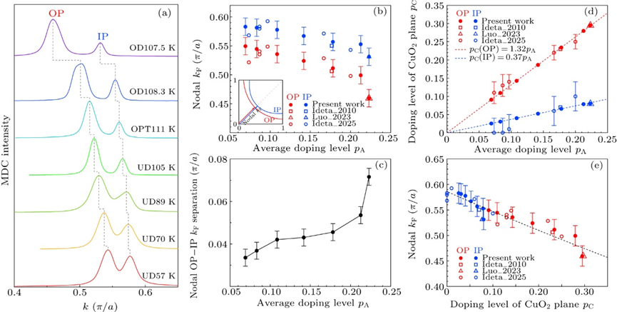
Fig. 3. Doping dependence of the nodal Fermi momentum and the charge distribution in OP and IP CuO2 planes in Bi2223. (a) MDCs at the Fermi level obtained from Fig. 2(b). (b), The nodal Fermi momentum kF of the OP (red symbols) and IP (blue symbols) bands obtained from (a) as a function of the average doping level (pA). The nodal Fermi momentum kF is defined in the inset of (b). (c), The nodal Fermi momentum difference between the OP and IP bands in our Bi2223 samples. (d), The charge distribution in OP (red symbols) and IP (blue symbols) CuO2 planes in Bi2223 with different doping levels. The doping levels on the OP CuO2 planes from the previous ARPES measurements are fitted by a linear line (red dashed line). Then the doping levels on the IP CuO2 planes are deduced (blue dashed line). The charge distribution in OP and IP CuO2 planes in our Bi2223 samples are determined based on the two lines. (e), The nodal Fermi momentum kF of the OP (red symbols) and IP (blue symbols) bands as a function of the doping level of their corresponding CuO2 planes (pC).
亮点文章
Momentum-dependent Anisotropy of the Charge Density Wave Gap in Quasi-1D ZrTe3-xSex (x=0.015)
Renjie Zhang(张任杰), Yudong Hu(胡裕栋), Yiwei Cheng(程以伟), Yigui Zhong(钟益桂), Xuezhi Chen(陈学智), Junqin Li(李俊琴), Kozo Okazaki, Yaobo Huang(黄耀波), Tian Shang(商恬), Shifeng Jin(金士锋), Baiqing Lv(吕佰晴), and Hong Ding(丁洪)
Chin. Phys. B, 2025, 34 (7): 077106
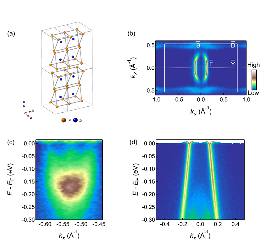
Fig. 1. Lattice and electronic structure of ZrTe3₋ₓSeₓ. (a) Quasi-one-dimensional lattice structure of ZrTe3₋ₓSex. (b) Fermi surface of ZrTe₀.₉₈₅Se₀․₀₁₅ plotted in the surface Brillouin zone. (c) Opening of the charge-density-wave (CDW) gap near the Fermi energy on the quasi-1D Fermi surface. (d) Absence of the CDW gap near the Fermi energy on the quasi-2D Fermi surface.
亮点文章
In-plane negative magnetoresistance and quantum oscillations in van der Waals antiferromagnet DyTe3
Qi Qi(齐琦), Senhao Lv(吕森浩), Ke Zhu(祝轲), Yaofeng Xie(谢耀锋), Guojing Hu(胡国静), Zhen Zhao(赵振), Guoyu Xian(冼国裕), Yechao Han(韩烨超), Yang Yang(杨洋), Lihong Bao(鲍丽宏), Xiao Lin(林晓), Hui Guo(郭辉), Haitao Yang(杨海涛), and Hong-Jun Gao(高鸿钧)
Chin. Phys. B, 2025, 34(7): 077305
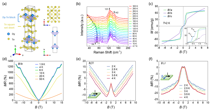
Fig. 4. (a) Crystal structure of DyTe3. Dy-Te block layer are sandwiched between square net sheets formed by Te atoms. (b) Typical temperature-dependent Raman spectra of DyTe3 single crystal from 300 K to 4.7 K, showing an obvious evolution of the peak corresponding to CDW. (c) Magnetization curve along the b-axis, showing two transitions with critical fields of 0.8 T and 1.1 T. (d) Normalized MR at various temperatures from 1.9 K to 50 K, showing a linear MR at low temperatures and SdH oscillations under high magnetic fields. (e), (f) Field dependence of MR as the field parallel to the current and as the field perpendicular to the current at T<TN, showing a transition as the field increasing.
亮点文章
Characterization of antisite defects and in-gap states in antiferromagnetic MnSb2Te4
Junming Zhang(张峻铭), Ming Xi(席明), Yuchong Zhang(张羽翀), Hang Li(李航), Jiali Zhao(赵佳丽), Hechang Lei(雷和畅), Zhongxu Wei(魏忠旭), and Tian Qian(钱天)
Chin. Phys. B, 2025, Vol. 34(7): 076801
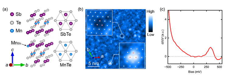
Fig. 1. Lattice structure and electronic state of MnSb2Te4. (a) Side view and top view of crystal structure of MnSb2Te4. A MnSb antisite defect is marked illustratively. (b) Atomically resolved STM topographic image of MnSb2Te4 (size: 25 × 25 nm2, VB = -0.55 V, It = 300 pA). Insert: Two types of antisite defects, which can be identified as dark triangles and bright dots. (c) Typical tunneling spectra taken at the defect of bright dot.
亮点文章
Zhongqiang Chen(陈中强), Zhe Wang(王喆), Kankan Xu(徐侃侃), Xu Zhang(张旭), Ruijie Xu(徐睿劼), and Xuefeng Wang(王学锋)
Chin. Phys. B, 2025, Vol. 34(7): 077401
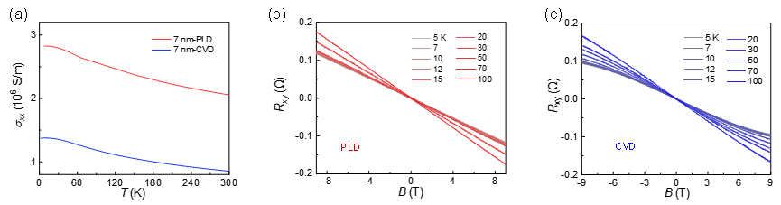
Fig. 1. (a) Temperature-dependent conductivity of the 7-nm-thick PtTe2 films grown by PLD (red curve) and CVD (blue curve), respectively. (b), (c) The Hall curves at various temperatures for the PtTe2 grown by PLD and CVD, respectively.
亮点文章
Bayesian phase difference estimation based on single-photon projective measurement
Xu-Hao Yu(余旭豪), Ying Wei(韦颖), Ran Yang(杨然), Wen-Hui Song(宋文慧), Yingning Miao(缪应宁), Wei Zhou(周唯), Xinhui Li(李新慧), Xiaoqin Gao(高小钦), Yan-Xiao Gong(龚彦晓), and Shi-Ning Zhu(祝世宁)
Chin. Phys. B, 2025, Vol. 34(7): 070305
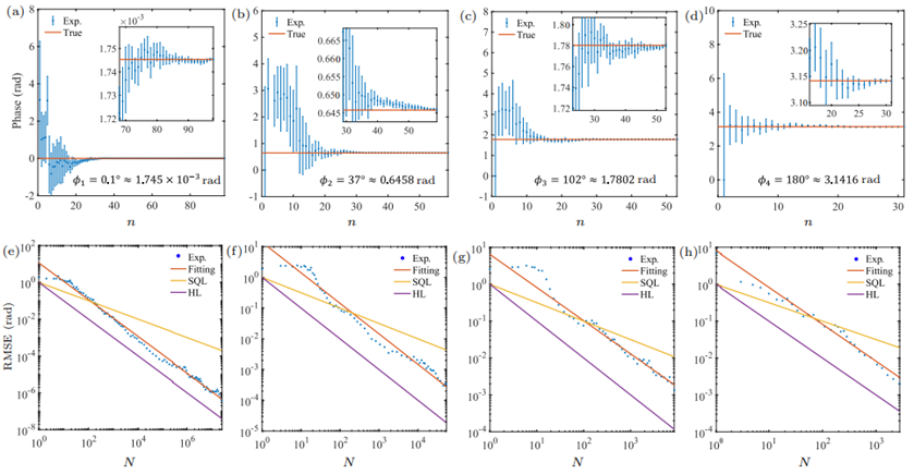
Fig. 3. Phase estimation process with different phase values. (a), (b), (c), and (d) are the estimated phases for rad,
rad,
rad, and
rad, respectively, with the corresponding RMSE plotted in (e), (f), (g), and (h). Here, n is the iteration number and N is the consumed resource number.

Instrumentation and Measurement
Computational Programs for Physics

Celebrating 30 Years of Chinese Physics B
Stephen J. Pennycook: A research life in atomic-resolution STEM and EELS
Recent progress on kagome metals and superconductors
Moiré physics in two-dimensional materials
Computational programs in complex systems
Quantum computing and quantum sensing
Structures and properties of materials under high pressure
Post-Moore era: Materials and device physics
States and new effects in nonequilibrium
Smart design of materials and design of smart materials
Superconductivity in vanadium-based kagome materials

https://iopscience.iop.org/journal/1674-1056
https://blog.sciencenet.cn/blog-3377544-1514669.html
上一篇:[转载]CPB封面文章 | 2025年第7期
下一篇:[转载]CPB2025年第10期文章目录-1
